Introduction
The field of micro- and nanoelectronics heavily relies on silicon semiconductors, whose performance can be significantly influenced by irradiation. Recent studies have shed light on the behavior of irradiated semiconductors, specifically silicon, and the mechanisms driving changes in their electrical conductivity. This blog post dives into the findings of Pagava et al. (2024) and related research, highlighting how high-energy particle irradiation and subsequent annealing processes affect the electrical properties of these materials.
Key Concepts in Irradiated Semiconductor Conductivity
Irradiating semiconductors, particularly silicon, introduces radiation defects (RDs) that modify the material’s physical and electrical properties. These RDs, including point defects, clusters, and nanoscale disordered regions, are formed through interactions with high-energy particles such as protons and electrons. Understanding the formation, evolution, and impact of these defects is crucial for advancing semiconductor technology.
Findings on Electrical Conductivity Mechanisms
Formation of Disordered Regions
Irradiated semiconductors experience the creation of highly conductive, nanosized disordered regions. These regions, surrounded by defective shells, act as capacitors, storing charge that can block current carriers. This phenomenon, known as the Coulomb blockade, results in decreased Hall mobility of charge carriers, as observed in both n-type and p-type silicon. The interplay between highly conductive inclusions and their transformation into low-conductivity regions underlies the observed changes in mobility.
Temperature and Annealing Effects
The effects of temperature and annealing on irradiated silicon are profound. Studies reveal:
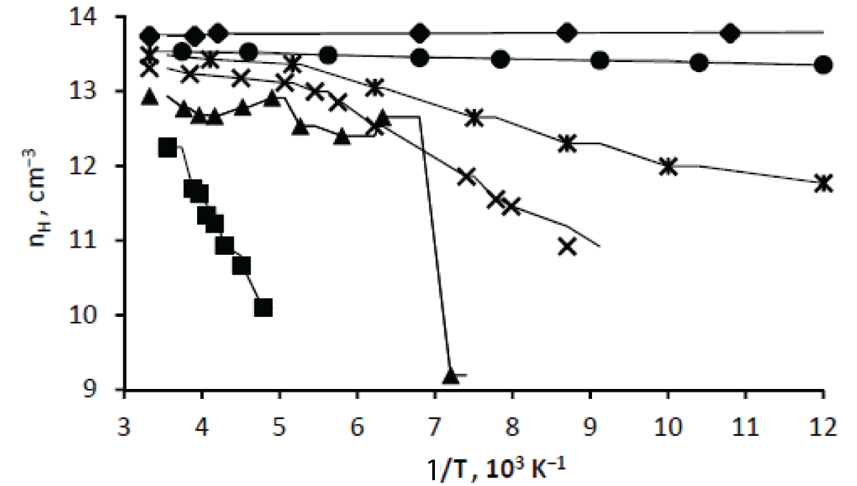
Hall Concentration Variations: Electron Hall concentration oscillates with temperature, influenced by the ionization of charged defect centers. Specific temperature ranges lead to deionization of A-centers, divacancies, and other defect states, impacting the conductivity.
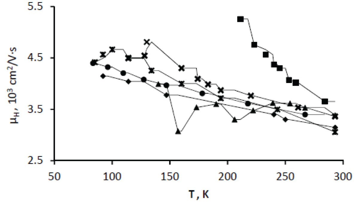
Mobility Trends: In irradiated samples, Hall mobility first increases with temperature due to decreased scattering from charged defects, only to decrease again as phonon scattering dominates at higher temperatures.
Recovery Post-Annealing: Annealing processes lead to the gradual recovery of electrical properties, as radiation-induced defects are neutralized or reorganized. Complete recovery, however, often requires high temperatures, such as 500 °C.
Implications for Semiconductor Applications
The study emphasizes the potential of irradiation as a tool for fine-tuning semiconductor properties. By manipulating irradiation doses, particle energies, and annealing protocols, researchers can achieve targeted modifications in material properties. This approach holds promise for applications in high-performance micro- and nanoelectronic devices.
Research Significance and Future Directions
The insights provided by Pagava et al. (2024) and complementary research open avenues for optimizing semiconductor materials through controlled irradiation. Future studies could focus on:
Enhancing theoretical models to predict the behavior of irradiated semiconductors under various conditions.
Exploring the impact of different dopants and impurity concentrations on defect formation and mobility.
Developing advanced experimental techniques to visualize and quantify nanoscale disordered regions and their electrical effects.
Conclusion
The exploration of irradiated semiconductors unveils a fascinating interplay between defect formation, temperature dynamics, and annealing. By leveraging these mechanisms, the semiconductor industry can advance towards more resilient and efficient materials, paving the way for innovations in electronics.
Tags: semiconductor, irradiation, nanotechnology, Hall mobility, electrical conductivity, microelectronics, defect formation, silicon research