
On how Doping with Atoms of Gadolinium and Scandium affects the Surface Structure of Silicon
Exploring the Impact of Gadolinium and Scandium Doping on Silicon Surface Structures
Silicon, the backbone of modern electronics, continuously undergoes innovation to meet the demands of advancing microelectronics. Recent studies highlight a groundbreaking technique for doping silicon with rare-earth elements like gadolinium (Gd) and scandium (Sc) to enhance its physical and electrical properties.
This post delves into the study “On How Doping with Atoms of Gadolinium and Scandium Affects the Surface Structure of Silicon,” authored by researchers at the National University of Uzbekistan. The paper, published in IgMin Research, introduces a novel low-temperature diffusion doping method and its impact on silicon’s structural and functional parameters.
Why Silicon Doping Matters
Doping introduces impurity atoms into silicon’s crystal lattice to alter its electrical and physical properties. Traditional high-temperature doping techniques have limitations such as surface erosion and alloy formation. The study addresses these challenges with a low-temperature diffusion doping method, paving the way for the development of advanced semiconductor devices.
Key Highlights of the Study
Uniform Cluster Distribution
The low-temperature diffusion technique ensures the uniform distribution of gadolinium and scandium clusters across the silicon bulk. Unlike high-temperature methods, it prevents surface degradation and silicide formation.Improved Thermostability and Radiation Resistance
Silicon doped with these rare-earth elements exhibits increased thermal and radiation stability, making it ideal for high-performance applications.Novel Physical Phenomena
The clustering of gadolinium and scandium atoms introduces unique properties, enabling new functionalities in microelectronics and optoelectronics.
Methodology
Low-Temperature Diffusion Doping Process
The study utilized a step-by-step approach:
- Preparation: Silicon samples were doped with gadolinium and scandium using evacuated quartz ampoules.
- Diffusion: Samples were subjected to controlled heating, gradually increasing temperatures to a peak of 1250°C.
- Post-Processing: Layers were etched and analyzed to determine the concentration and distribution of dopant clusters.
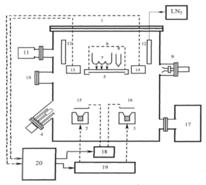 Figure 1: Analytical growth chamber: 1, 2, 3 – electron beam evaporators; 4-effusion source; 5-sample; 6-manipulator; 7-heater; 8-thermocouple; 9-electron gun of the fast electron diffractometer; 10-fluorescent screen; 11 quadrupole gas analyzers; 12-cryopanel; 13, 14- deposition rate sensors (quartz); 15, 16 dampers; 17-ion pump; 18-control dampers with a servo drive; 19-power supplies of electron-beam evaporators; 20-processor unit.
Techniques Used:
- Infrared Microscopy (INFRAM-I): For analyzing dopant distribution across the silicon bulk.
- Hall Effect Measurements: To evaluate electrical parameters.
- Autoradiography and Microprobe Analysis: For structural insights.
Findings
- At low temperatures, diffusion primarily occurs via interstitial mechanisms, resulting in a stable cluster formation.
- The process significantly reduces energy consumption and eliminates surface erosion.
Impact on Electrical and Thermal Properties
Lifetime of Minority Charge Carriers
Doped silicon samples showed stable minority carrier lifetimes across a wide temperature range, critical for device reliability.Radiation Resistance
Gadolinium-doped samples retained electrical stability even after exposure to γ-irradiation, demonstrating their robustness for radiation-heavy environments.
- Cluster Formation and Functionality
Clusters formed through this method can act as “getter agents,” reducing impurities and defects in silicon.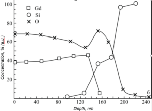 Figure 2: Concentration profiles of Gd in silicon samples not subjected to high-temperature annealing.
Applications in Advanced Electronics
The findings open up possibilities for new semiconductor applications:
- Microelectronics: Enhanced stability and reduced defect levels improve transistor performance.
- Optoelectronics: The introduction of rare-earth clusters enables novel light-emitting properties.
- Radiation-Resistant Devices: Ideal for aerospace and nuclear applications.
Comparative Analysis with Traditional Methods
Advantages of Low-Temperature Diffusion
- Reduced Process Time: 2-2.5 times faster than conventional methods.
- Lower Energy Consumption: Significant reduction in operational costs.
- Minimal Surface Damage: No erosion or silicide formation observed.
Limitations Addressed
High-temperature techniques often lead to:
- Alloy formation on the surface.
- Uneven distribution of impurity atoms.
- Thermal stresses and defects.
Future Research Directions
The study sets the stage for further exploration:
- Optimizing Cluster Control: Developing techniques to manipulate cluster size and distribution.
- Exploring Other Rare-Earth Elements: Investigating their potential for silicon doping.
- Device Integration: Applying doped silicon in real-world electronic devices.
Figure 3: Micrograph of the bulk of a silicon sample into which gadolinium was diffused using conventional high-temperature diffusion technology.
Conclusion
The innovative doping method presented in this study not only enhances the functionality of silicon but also introduces sustainable and efficient manufacturing practices. The uniform clusters of gadolinium and scandium provide unprecedented control over silicon’s properties, marking a significant milestone in semiconductor research.
References
- Egamberdiev BE, et al. On How Doping with Atoms of Gadolinium and Scandium Affects the Surface Structure of Silicon. IgMin Research. PDF.
- DOI: 10.61927/igmin206.
- Additional insights: IgMin Research.